
After studying and learn about DS12C887 through internet and Lecture slide. I start to make the schematic using proteus.
This circuit is interfacing LCD 16x2 and RTC with 8051.
LCD is connected to port 2 and sent 8-bit data.
RTC is set to send data at PORT 0 .
Port 1 and 3 is set to sent input signal ti set the time.
This program use External interrupt 0 and 1 for setting the time and alarm.
When the interrupt is active, 8051 will stop the operation and ready to set time or alarm.
DS12C887 Real Time Clock:
This IC is used most of the applications to provide accurate time and date. This IC provides the time in both 12 hour mode and 24 hour mode. This IC also provides calendar components day, month and year. This RTC uses internal lithium battery to keep the time and date updated when power is failed. This IC has 128 bytes of RAM memory. In these 128 bytes of RAM 14 bytes are used for time, date and registers. Remaining 114 bytes are used to store general purpose data.
The control registers of RTC are accessible only when the power is applied from external source. This IC requires more than 4.25V power supply and the control registers are accessible after 200ms when external power is supplied.
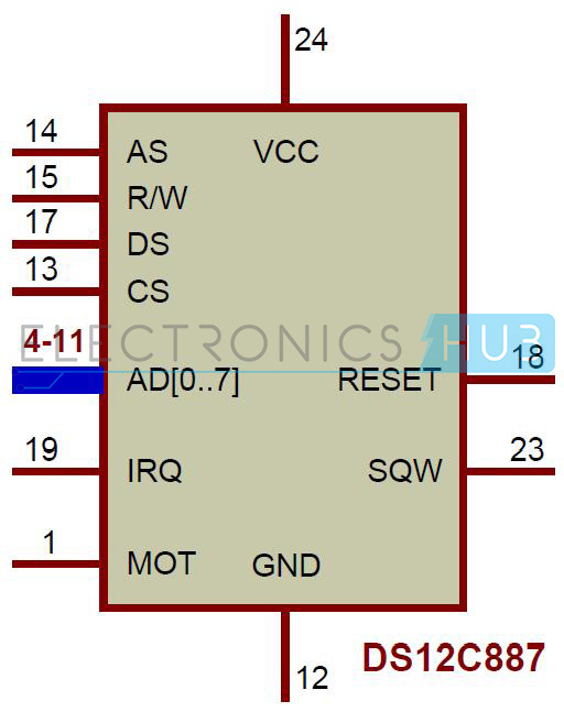
DS12C887 IC
Pin Description:
- MOT: It is a bus type selection pin used to select between Intel and Motorolabus types. This pin is connected to VCC to select Motorola bus type and connected to GND or unconnected to select Intel bus type.
- 2, 3: Unused pins
- 4 – 11 (AD0 – AD7): These pins are bidirectional address and data lines of RTC. On these pins address is present in the first portion of cycle and data is present in the second portion of bus cycle.
- 12 (GND): This pin is connected to Ground.
- 13 (CS): This pin must be low to access the chip during read and write operations.
- 14 (AS): The high pulse on this pin is used to demultiplex the data and address.
- 15 (R/W): This pin is used for read or writes operations.
- 16: Unused pin
- 17 (DS): This is a Data Strobe pin.
- 18 (RESET): The low pulse on this pin resets all the flags and interrupts but it does not affects time and date.
- 19 (IRQ): Thisis active low pin used as an interrupt input to the controller.
- 20 – 22: Unused pins
- 23 (SQW): Used to generate square wave with predefined frequencies
- 24 (VCC): This pin is connected 5V supply
RTC Address Map:
This RTC has 128 bytes of RAM with addresses 00H – 07H. The first ten locations (00 – 09) are used for clock, calendar and alarm data. 0A – 0D address locations are used for status and control registers. Remaining address locations are used to for general data. The following table shows the address locations for clock, calendar and alarm.
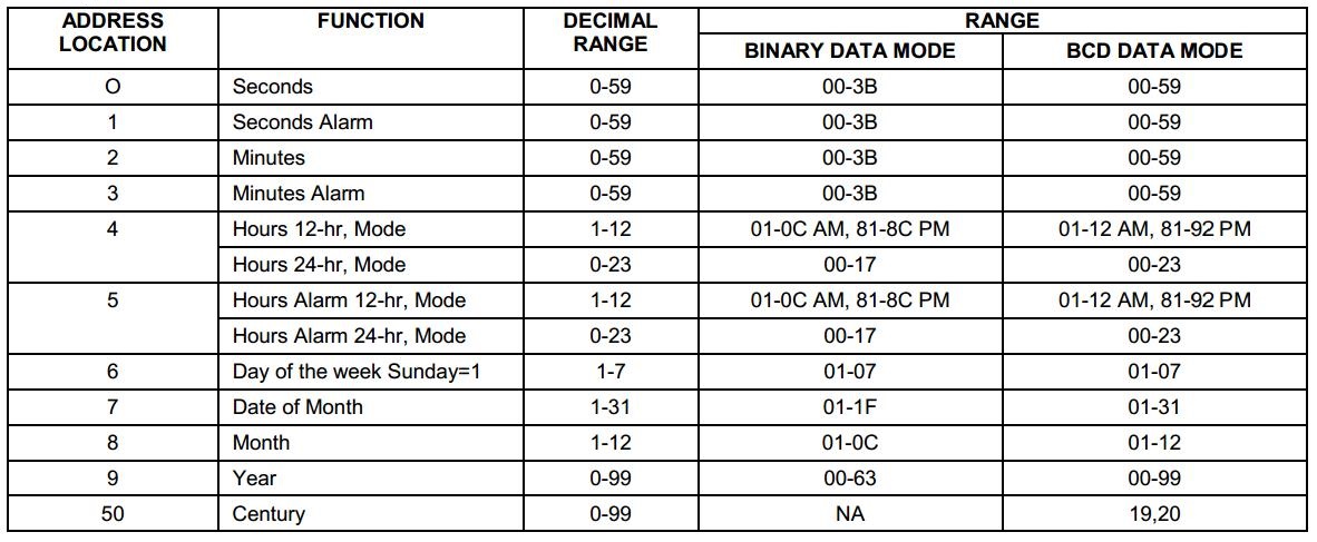
Address Locations for Time, Date and Alarm
This IC has 4 control and status registers namely register A, register B, Register C, register D. We need to configure all these registers to get the accurate time and date. In order to configure these registers go through the DS12C887 Datasheet


0 comments:
Post a Comment